Abstract
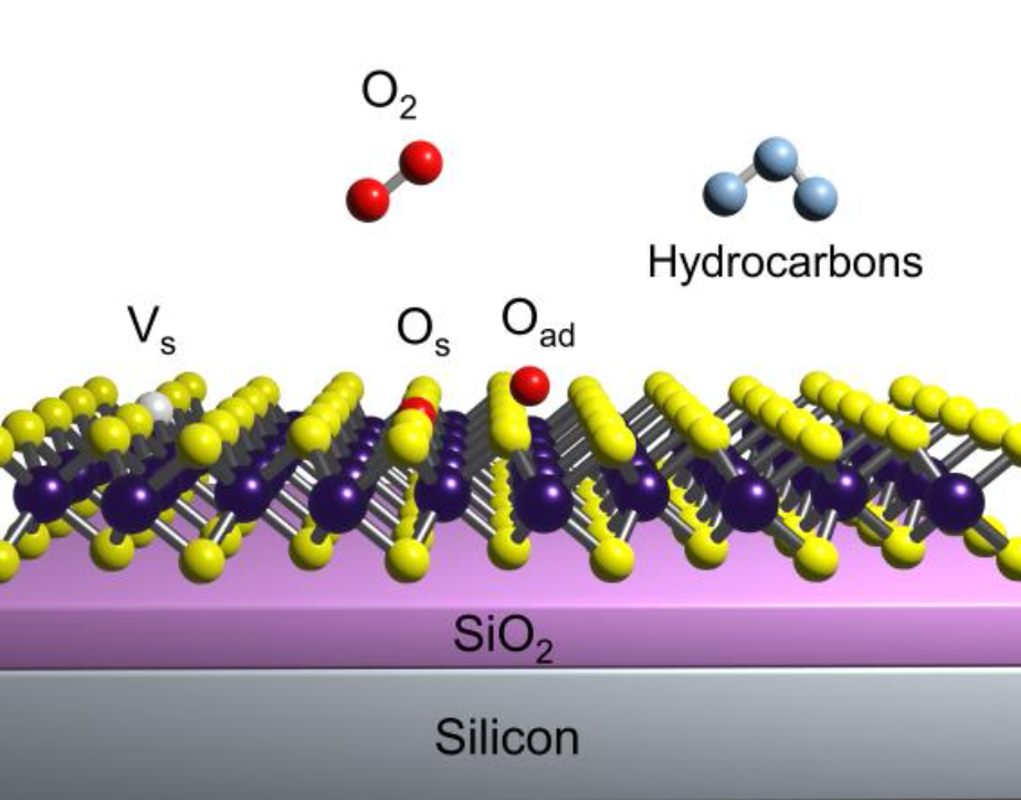
2D transition metal dichalcogenides (TMDs) are leading materials for next-generation optoelectronics, but fundamental problems stand enroute to commercialization. These problems include firstly, the widely debated defect and strain-induced origins of intense low-energy broad luminescence peaks (L-peak) observed at low temperatures. Secondly, role of oxygen in tuning properties via chemisorption and physisorption is intriguing but challenging to understand. Thirdly, physical understanding of benefits of hBN encapsulation is inadequate. Using a series of samples, we decouple contributions of oxygen, defects, adsorbates, and strain on optical properties of monolayer MoS2. Defect-origin of L-peak is confirmed by temperature and power-dependent photoluminescence (PL) measurements, with a dramatic redshift ~130 meV for oxygen-assisted chemical vapour deposition (O-CVD) samples (c.f. exfoliated). Anomalously, O-CVD samples show high A-exciton PL at room temperature (c.f. exfoliated), but reduced PL at low temperatures, attributed to strain-induced direct-to-indirect bandgap-crossover in low-defect O-CVD MoS2. These observations are consistent with our density functional theory calculations, and supported by Raman spectroscopy. In exfoliated samples, charged O-adatoms are identified as thermodynamically favourable defects, and create in-gap states. Beneficial effect of encapsulation originates from reduction of charged O-adatoms and adsorbates. This experimental-theoretical study uncovers the type of defects in each sample, enables an understanding of the combined effect of defects, strain and oxygen on band structure, and enriches understanding of effects of encapsulation. This work proposes O-CVD for creating high-quality materials for optoelectronics.
